My first SMT PCB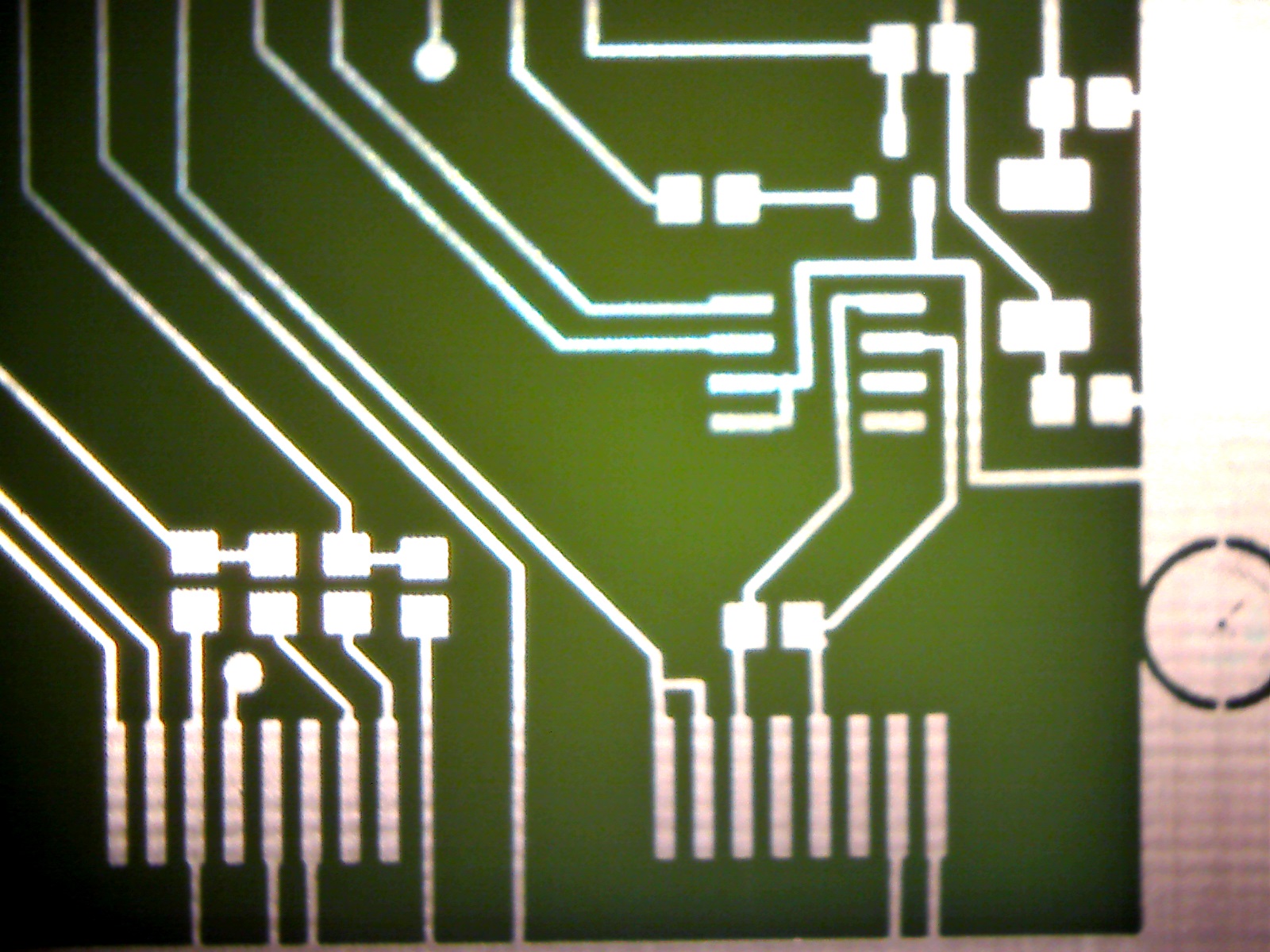 (right-click and "view image" to see it with full detail) i was worried - but for no reason. it was easy. i endured hours of painful, complicated videos and articles about how to make your own PCB. even looked hard into converting a laser printer to print directly onto a PCB for a better quality etch resist image. i was worred about the quality of my image, the exposure time, that i was not able to print it mirrored to have the print side down, and the tiny-ness of everything SMT (surface mount). all for naught. i was amazed at the results. so if you're considering making a PC board, "just do it." here's how i did it.... Update!!ouch. must have been beginner's luck. had a couple bad batches. 2nd board, the developer washed all the resist off in seconds. and a couple batches had little resist left, so traces were sketchy. but found the secret to the developing... don't agitate. maybe a little towards the end. silly me. i was sloshing it around like i did the acid while etching. the developer is meant to just sit there. i also lessened the exposure time and diluted the developer a bit.CAD software - lay it outwhew. what a mess. so many to choose from and most with serious limitations. even tried the famous Eagle. good grief. be prepared to spend days reading the manual. there are a dozen steps just to get to laying out the schematic.i really like PCBWeb. i found it on the digikey.com site and it's tied to their parts inventory, and to a few board production houses that i might use someday. it's a bit strange at times. had a devil of a time drawing two traces on the bottom side of the board. and other things tend to not work (the way i think they should). but for just diving in and getting things going, it's just natural. right in front of you on the main screen are "schematic" and "pcboard" tabs. it's like they knew ahead of time that's what i wanted to do instead of hiding it behind a dozen menus. and there's a collection of short videos help get you going. i was even adding parts to the library in no time. some hints. when you start your schematic, right click on it and change some properties, like size to 'letter' instead of 'humongous'. so sweet. after you draw the schematic, click on PC board. adjust the size of your board by clicking, then moving each corner. (don't drag as that will drag the whole outline. oops.) you'll need to look below the outline to find your parts, then move them onto the board. *your* board. so cool. if you're in schematic mode and go to the File menu, it will print your schematic it to a PDF file. same thing if you're in pc board mode. it prints the board to a PDF file, actual size. to use that for etching your own board, de-select silkscreen, soldermask, and text. it will print in red. i worried that it wouldn't be dark enough. and i can see the hatchmarks from the printer as it greyscaled the red, but it's minor compared to the quality of the board. i also worried that i couldn't mirror it to expose it ink-side-down. but that also worked out just fine. a bit tricky finding transparency film to print on, but even that turned up. make sure you use printer/copier film. the "write on" film won't take the heat of the laser/copier fuser. Make your boardi am using "positive presensitized" boards from MG Chemicals. they really know what they're doing. get a bottle of their Developer too. i bought their Photofabrication kit 416-K but only used the developer and a board from it. didn't even use the foam brushes as the resist went away quickly on its own in the developing, and just rocking the pan back and forth was plenty good for the etching.anyway, take the glass out of a picture frame (not your wedding pictures) to press your image against their sensitized board. expose for 8-10 min under a florescent desk lamp per their instructions. dilute their developer, put in your board, and watch the green resist disappear from the exposed areas, leaving your traces still green. wow. Etch itget some Muriatic acid from a hardware store (paint section) and some hydrogen peroxide from pharmacy or grocery store. mix it 1 part acid to 2 parts hydrogen peroxide. 3 oz acid and 6 oz hydrogen peroxide was plenty. soon you'll see the bare board appearing where the copper used to be. don't even try ferric choride. you have to heat it up for it to work, and it's dark so you can't see your beautiful board taking shape.Just do itthe exposure times are not critical. i did 3 copies (panels) of my 2x3" board at once, exposing one part for 8, another 10, and another 12 min. they all worked fine, tho the 10min was best. you can see the greyscale hashmarks on the traces and on the solid areas, but there's still plenty of copper there.the process is really a lot more forgiving than the videos and articles made it out to be. so... what are you waiting for? dave allen Reyware LLC |